- 您现在的位置:买卖IC网 > Sheet目录3871 > PIC18F1230T-I/ML (Microchip Technology)IC PIC MCU FLASH 2KX16 28QFN
PIC18F1230/1330
2009 Microchip Technology Inc.
DS39758D-page 185
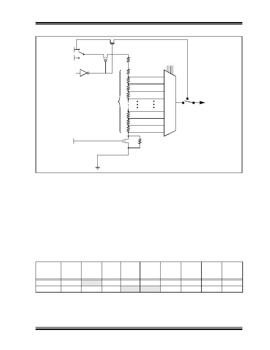
FIGURE 18-1:
COMPARATOR VOLTAGE REFERENCE BLOCK DIAGRAM
18.2
Voltage Reference Accuracy/Error
The full range of voltage reference cannot be realized
due to the construction of the module. The transistors
on the top and bottom of the resistor ladder network
reference source rails. The voltage reference is derived
from the reference source; therefore, the CVREF output
changes with fluctuations in that source. The tested
absolute accuracy of the voltage reference can be
18.3
Operation During Sleep
When the device wakes up from Sleep through an
interrupt or a Watchdog Timer time-out, the contents of
the CVRCON register are not affected. To minimize
current consumption in Sleep mode, the voltage
reference should be disabled.
18.4
Effects of a Reset
A device Reset disables the voltage reference by clearing
bit, CVREN (CVRCON<7>). This Reset selects the high-
voltage range by clearing bit, CVRR (CVRCON<5>). The
CVR value select bits are also cleared.
TABLE 18-2:
REGISTERS ASSOCIATED WITH COMPARATOR VOLTAGE REFERENCE
16-t
o-1
MUX
CVR3:CVR0
8R
R
CVREN
CVRSS = 0
AVDD
VREF+
CVRSS = 1
8R
CVRSS = x
AVSS
R
16 Steps
CVRR
CVREF
CVREN = 0
CVREN = 1
Name
Bit 7
Bit 6
Bit 5
Bit 4
Bit 3
Bit 2
Bit 1
Bit 0
Reset
Values
on Page:
CVRCON
CVREN
—
CVRR
CVRSS
CVR3
CVR2
CVR1
CVR0
CMCON
C2OUT
C1OUT
C0OUT
—
CMEN2
CMEN1
CMEN0
Legend:
Shaded cells are not used with the comparator voltage reference.
发布紧急采购,3分钟左右您将得到回复。
相关PDF资料
PIC18F1230T-I/SO
IC PIC MCU FLASH 2KX16 18SOIC
PIC18F1330T-I/ML
IC PIC MCU FLASH 4KX16 28QFN
PIC18F65J50T-I/PT
IC PIC MCU FLASH 16KX16 64TQFP
PIC18F83J11T-I/PT
IC PIC MCU FLASH 4KX16 80TQFP
PIC16LF627-04/P
IC MCU FLASH 1KX14 COMP 18DIP
PIC18F86J55T-I/PT
IC PIC MCU FLASH 48KX16 80TQFP
PIC18F43K22-I/MV
MCU PIC 8KB FLASH 40QFN
PIC16C55A-04I/P
IC MCU OTP 512X12 28DIP
相关代理商/技术参数
PIC18F1230T-I/SO
功能描述:8位微控制器 -MCU 4KB Flash 256 RAM RoHS:否 制造商:Silicon Labs 核心:8051 处理器系列:C8051F39x 数据总线宽度:8 bit 最大时钟频率:50 MHz 程序存储器大小:16 KB 数据 RAM 大小:1 KB 片上 ADC:Yes 工作电源电压:1.8 V to 3.6 V 工作温度范围:- 40 C to + 105 C 封装 / 箱体:QFN-20 安装风格:SMD/SMT
PIC18F1230T-I/SS
功能描述:8位微控制器 -MCU 4KB Flash 256 RAM RoHS:否 制造商:Silicon Labs 核心:8051 处理器系列:C8051F39x 数据总线宽度:8 bit 最大时钟频率:50 MHz 程序存储器大小:16 KB 数据 RAM 大小:1 KB 片上 ADC:Yes 工作电源电压:1.8 V to 3.6 V 工作温度范围:- 40 C to + 105 C 封装 / 箱体:QFN-20 安装风格:SMD/SMT
PIC18F1320-E/ML
功能描述:8位微控制器 -MCU 8KB 256 RAM 16 I/O RoHS:否 制造商:Silicon Labs 核心:8051 处理器系列:C8051F39x 数据总线宽度:8 bit 最大时钟频率:50 MHz 程序存储器大小:16 KB 数据 RAM 大小:1 KB 片上 ADC:Yes 工作电源电压:1.8 V to 3.6 V 工作温度范围:- 40 C to + 105 C 封装 / 箱体:QFN-20 安装风格:SMD/SMT
PIC18F1320-E/P
功能描述:8位微控制器 -MCU 8KB 256 RAM 16 I/O RoHS:否 制造商:Silicon Labs 核心:8051 处理器系列:C8051F39x 数据总线宽度:8 bit 最大时钟频率:50 MHz 程序存储器大小:16 KB 数据 RAM 大小:1 KB 片上 ADC:Yes 工作电源电压:1.8 V to 3.6 V 工作温度范围:- 40 C to + 105 C 封装 / 箱体:QFN-20 安装风格:SMD/SMT
PIC18F1320-E/SO
功能描述:8位微控制器 -MCU 8KB 256 RAM 16 I/O RoHS:否 制造商:Silicon Labs 核心:8051 处理器系列:C8051F39x 数据总线宽度:8 bit 最大时钟频率:50 MHz 程序存储器大小:16 KB 数据 RAM 大小:1 KB 片上 ADC:Yes 工作电源电压:1.8 V to 3.6 V 工作温度范围:- 40 C to + 105 C 封装 / 箱体:QFN-20 安装风格:SMD/SMT
PIC18F1320-E/SS
功能描述:8位微控制器 -MCU 8KB 256 RAM 16 I/O RoHS:否 制造商:Silicon Labs 核心:8051 处理器系列:C8051F39x 数据总线宽度:8 bit 最大时钟频率:50 MHz 程序存储器大小:16 KB 数据 RAM 大小:1 KB 片上 ADC:Yes 工作电源电压:1.8 V to 3.6 V 工作温度范围:- 40 C to + 105 C 封装 / 箱体:QFN-20 安装风格:SMD/SMT
PIC18F1320-H/ML
功能描述:8位微控制器 -MCU 8KB FL 256RAM 16 I/O RoHS:否 制造商:Silicon Labs 核心:8051 处理器系列:C8051F39x 数据总线宽度:8 bit 最大时钟频率:50 MHz 程序存储器大小:16 KB 数据 RAM 大小:1 KB 片上 ADC:Yes 工作电源电压:1.8 V to 3.6 V 工作温度范围:- 40 C to + 105 C 封装 / 箱体:QFN-20 安装风格:SMD/SMT
PIC18F1320-H/P
功能描述:8位微控制器 -MCU 8KB FL 256RAM 16 I/O RoHS:否 制造商:Silicon Labs 核心:8051 处理器系列:C8051F39x 数据总线宽度:8 bit 最大时钟频率:50 MHz 程序存储器大小:16 KB 数据 RAM 大小:1 KB 片上 ADC:Yes 工作电源电压:1.8 V to 3.6 V 工作温度范围:- 40 C to + 105 C 封装 / 箱体:QFN-20 安装风格:SMD/SMT